
This semester at school, I took Advanced Computer Architecture. This has been my favorite class in college so far. The class dives deeper into topics from the regular Computer Architecture course, especially the parts that are hand-waved over as being too complicated.
The class is project-based (mostly) and had 2 large-sized projects. One was creating an out-of-order CPU in SystemVerilog, which I'll dive into in another blog. The other was anything we wanted to do (so long as the instructor approved it). My project was implementing the CHIP-8 and then GameBoy in SystemVerilog.
The CHIP-8 part was initially easy, as I had previously written a CHIP-8 emulator in C. My first stab at doing it in SV was done early in the semester before I was too familiar with SV and how to write it properly. The code resembled my C code, having one large case statement that would use blocking assignments to complete instructions. I used Verilator to simulate and test my design. Verilator was very nice as I could do FFI (Verilator calls it DPI) to talk to C++ code from my SV code. This allowed me to use SDL2 to take user input and to display the CHIP-8's screen on my laptop. I managed to get a fully working version of it done in a few days.
After this, I was able to borrow an FPGA from my instructor and set out to run my CHIP-8 on real hardware. I ordered a ST7920 LCD display, a buzzer, and a 16 key keypad off of Amazon the next day.
The most time-consuming part of this project so far was interfacing with the ST7920 LCD I ordered. The display has 2 modes for data transmission: 8/4 pin parallel, and serial. The specification for the parallel interface seemed to be the most straightforward, so I went ahead with implementing my driver with that.
The ST7920 has a fairly straightforward interface for drawing to the screen. It works by sending 8-bit instructions to the display controller. You first send a few initialization instructions to clear the display's memory and reset its state. After that you can select a mode (text or graphics). Both modes work similarly to where you set the position of the cursor on the screen and then send instructions that write pixels or text to that coordinate and then advances the coordinate by one.
I ran into trouble where I couldn't get anything to show up. Not even a simple "Hello World". To troubleshoot, I borrowed a friend's Arduino Mini which has proper drivers written for it for interfacing with the LCD. After hooking the display up to it, it also couldn't draw anything! It wasn't until I tried running it in serial mode that it worked. As it turns out, some manufacturers solder capacitors on the back that can disable certain features of the display (such as parallel mode), and my display's manufacturer had done just that. For this reason, I'd highly recommend buying from a big-name seller of electronic components such as Adafruit instead of random Amazon sellers.
Now that I knew that only the serial interface worked, I had to rewrite my driver to use it. This meant instead of putting all 8 bits of an instruction onto 8 pins at once, I'd have 2 pins: a clock and a data pin. In order to send an 8 bit instruction, I'd send a clock signal and set the data pin to either 1 or 0 based on whether the nth bit in my instruction would be a 1 or 0. There are additional device-specific characteristics of the ST7920's serial interface described in the above linked datasheet, but they're not relevant to getting the general idea of SPI (Serial Parallel Interface).
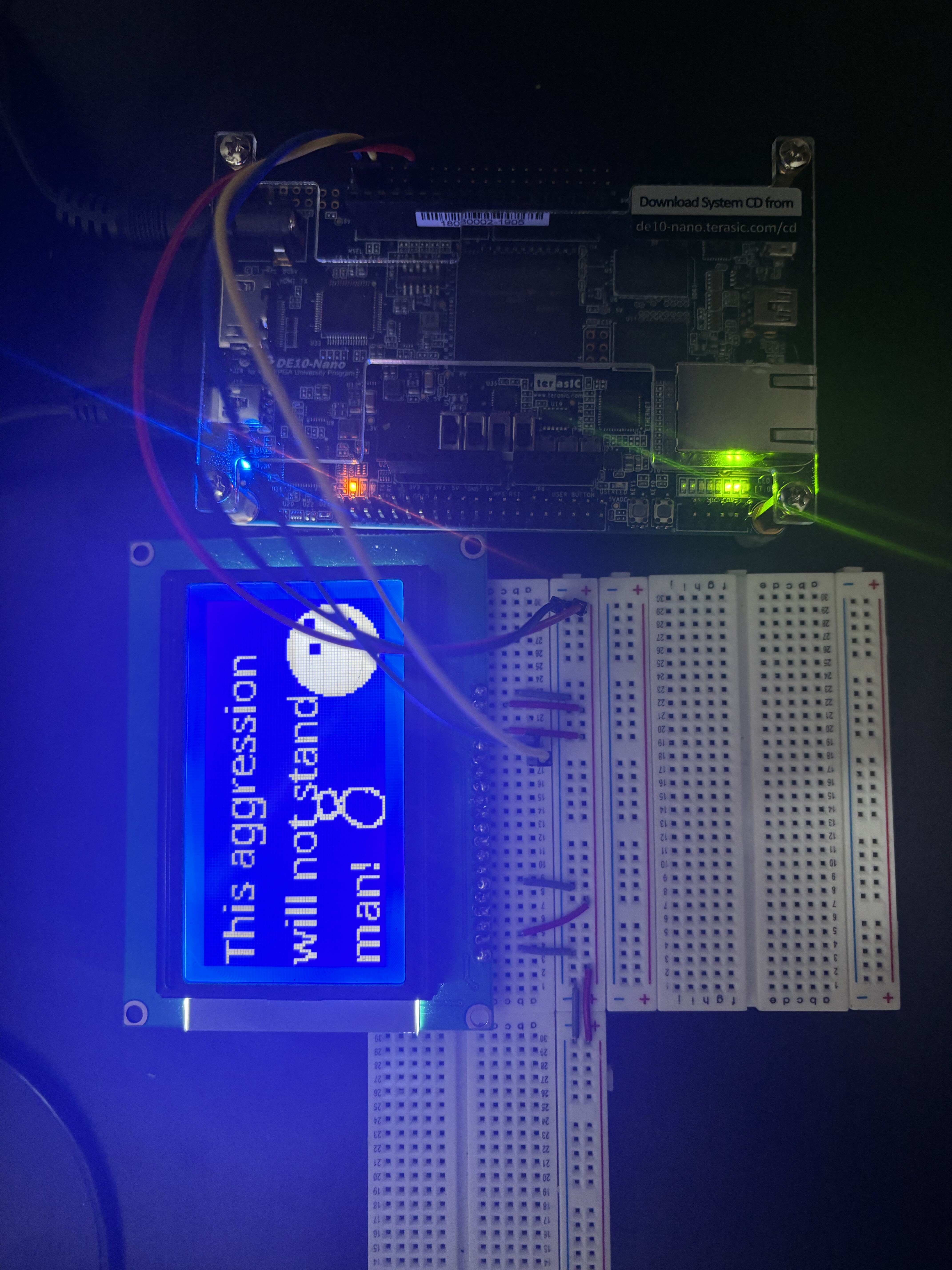
I implemented a serial driver with a little demo screen (see above image), and then modified the code to accept a block of memory of which it would then draw out to the display. This left me with a general-purpose ST7920 serial driver! Implementing a serial driver for this display gave me a good amount of experience in dealing with timing outside of simulations. It also taught me about debouncing and metastability.
The driver is hosted on GitHub here.
With my display driver finally done, I decided to try to hook my CHIP-8 code up to it and run it on the FPGA. I was really excited to actually run something on hardware. Then the build time started climbing and Intel Quartus crashed. I knew that this was a sign that I messed up. Through other projects in the class I learned a bit about Verilog and HDL best practices and knew that my giant blocking assignment switch statement would not run well, even if it would compile.
Rewriting the CHIP-8 to work in a way that's more consistent with how processors actually work and not how emulators work was fairly easy as I had done similar work previously. To do so, I turned the processor into a state machine where there was a state for each of the traditional 5 stages of the classic RISC pipeline. Each state would do what it needed to do and then move it into the next state. This design actually made logic very simple as I was able to combine the functionality for a lot of instructions. For example, a register to register load and an immediate to register load could use the same writeback logic, as by that stage they would be loading bits into a register. I didn't make it pipelined or do any fancy optimizations, mostly due to the fact that the CHIP-8 is supposed to run at ~480 Hz. It also wasn't in the scope of this project, as this was more about learning how different parts of a computer interact and how real-world ISA implementations are done.
At this point, I had a working CHIP-8 implemented in hardware sans a buzzer and user input. These parts I was able to knock out fairly quickly. The buzzer was dead simple, I just set its positive pin to high whenever the sound timer was greater than zero. The keypad was a little more challenging, but much simpler than the display. The keypad has 8 pins that are split between 4 column pins and 4 row pins. The FPGA sets 1 column pin to low and the rest to high on every clock cycle and reads the output from the row pins to determine which key is pressed. For instance if the first column pin was the one the FPGA had set to low, and then the FPGA read that the first row pin was outputting high, it would know that the pressed key was at coordinate (1,1) (i.e. the first key).
And after doing all of that, we can play Tetris!
The source code for yayacemu is hosted here. The CHIP-8 emulator I wrote in C was called yacemu (Yet Another Chip-8 Emulator), and the naming for this is yayacemu (Yet Another Yet Another Chip-8 Emulator).
I started writing the GameBoy implementation around the same time as I got the FPGA. As such, it's code structure heavily mirrored that of my first attempt at the CHIP-8's. For the project, I made no commitments to running it on an FPGA, and much of the GameBoy is implemented, so I'm pushing forward with keeping that structure. So far, the GameBoy can successfully run the bootrom, draw the background layer to the display, and run a little bit of the Tetris ROM (not enough to show anything yet).
The emulator booting!